-
Applied Materials’ New eBeam Metrology System Paves the Way to High-NA EUV Lithography
Источник: Nasdaq GlobeNewswire / 28 фев 2023 07:35:54 America/New_York
- New VeritySEM® 10 system delivers industry-leading resolution and imaging speed to help chipmakers accelerate process development and maximize yield in high-volume manufacturing
SANTA CLARA, Calif., Feb. 28, 2023 (GLOBE NEWSWIRE) -- Applied Materials, Inc. today introduced a new eBeam metrology system specifically designed to precisely measure the critical dimensions of semiconductor device features patterned with EUV and emerging High-NA EUV lithography.
Chipmakers use CD-SEMs (critical dimension scanning electron microscopes) to take sub-nanometer measurements of patterns once a lithography scanner transfers them from a mask to a photoresist. These measurements continuously calibrate lithography process performance to ensure the patterns are correct before they are etched into the wafer. CD-SEMs are also used after etch to correlate intended patterns with on-wafer results. CD-SEMs thereby help control the etch process and enable a feedback loop between lithography and etch that gives engineers highly correlated data sets for holistic process tuning.
Measuring the critical dimensions of semiconductor device features becomes more challenging as photoresists get thinner with EUV and especially High-NA EUV. To capture high-resolution images that provide accurate, sub-nanometer measurements, the CD-SEM must be able to precisely apply a narrow eBeam to the small area occupied by the extremely thin photoresist. eBeam energy interacts with photoresists, and if the landing energy is too high, the resist will shrink, distorting the pattern and creating errors. Conventional CD-SEMs cannot produce beams narrow enough to create high-resolution images at landing energies low enough to minimize interactions with the delicate High-NA photoresist.
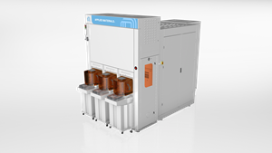
Introducing the VeritySEM® 10 CD-SEM Metrology System
Applied’s new VeritySEM 10 system features a unique architecture that enables low landing energy at 2X better resolution compared to conventional CD-SEMs. It also provides a 30-percent faster scan rate to further reduce interaction with the photoresist and increase throughput. The system’s industry-leading resolution and scan rate provide improved control of EUV and High-NA EUV lithography and etch processes to help chipmakers accelerate process development and maximize yield in high-volume manufacturing.
The VeritySEM 10 system is also being adopted by chipmakers for critical dimension metrology applications in 3D designs, including Gate-All-Around (GAA) logic transistors and 3D NAND memories, where the system’s back-scattered electrons enable high-resolution imaging of deep structures. Among the applications for GAA chips, the VeritySEM 10 is being used to measure and characterize the selective epitaxy process which is key to transistor performance. For 3D NAND memories, the system provides a large field of view and high depth of focus to measure entire staircase interconnect structures and help tune etch process recipes.
“The VeritySEM 10 system is a breakthrough in CD-SEM technology that solves the metrology challenges of major technology inflections that will shape the industry in the years ahead,” said Keith Wells, Group Vice President of Imaging and Process Control at Applied Materials. “The system’s unique combination of low landing energy, high resolution and faster imaging speed helps pave the way to High-NA EUV, Gate-All-Around transistors and high-density 3D NAND.”
The VeritySEM 10 system is receiving strong commercial interest from leading logic and memory customers, with more than 30 systems shipped over the past year. Multiple customers have selected the system as the development tool of record for GAA transistors. All leading 3D NAND customers have chosen the system as the development and process tool of record, and multiple DRAM customers have selected it as the process tool of record.
Additional information about Applied’s VeritySEM 10 system will be discussed at the company’s “New Ways to Shrink: Advanced Patterning Products Launch” event being held today.
About Applied Materials
Applied Materials, Inc. (Nasdaq: AMAT) is the leader in materials engineering solutions used to produce virtually every new chip and advanced display in the world. Our expertise in modifying materials at atomic levels and on an industrial scale enables customers to transform possibilities into reality. At Applied Materials, our innovations make possible a better future. Learn more at www.appliedmaterials.com.Contact:
Ricky Gradwohl (editorial/media) 408.235.4676
Michael Sullivan (financial community) 408.986.7977A photo accompanying this announcement is available at https://www.globenewswire.com/NewsRoom/AttachmentNg/252546cc-8fce-4349-a3e3-151ada434102
The photo is also available at Newscom, www.newscom.com, and via AP PhotoExpress.

- New VeritySEM® 10 system delivers industry-leading resolution and imaging speed to help chipmakers accelerate process development and maximize yield in high-volume manufacturing
